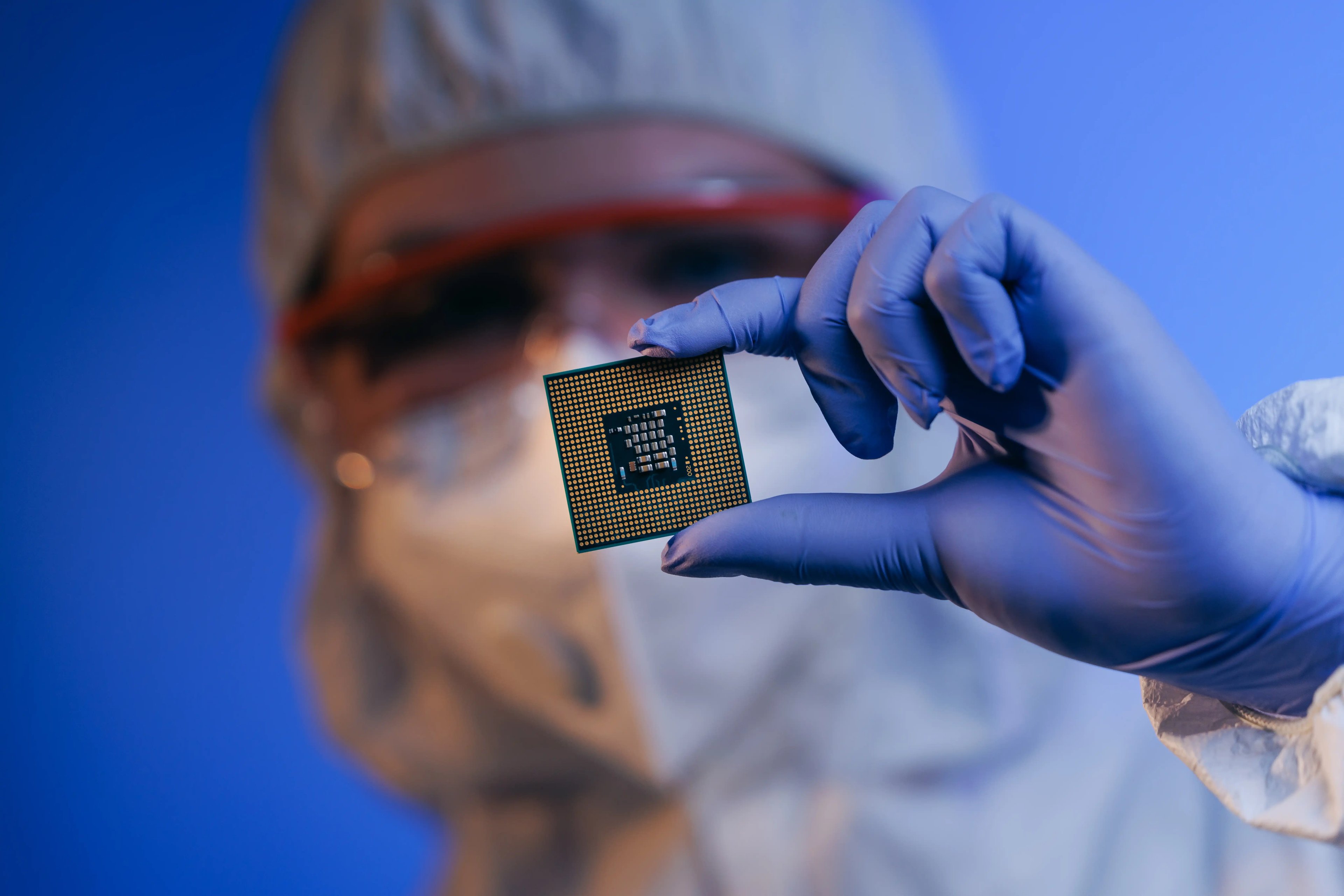
Semiconductors sit inside almost everything that uses electricity, from smartphones and cars to data centers and medical equipment. They are made by building microscopic structures layer by layer on thin silicon wafers, using heat, chemicals, light, and extreme precision. For that to work, the factory itself must behave like a precision instrument.
Before a wafer ever reaches a tool, before a single process step is qualified, the environment around it must already be stable. Air temperature is controlled to thousandths of a degree. Humidity is tightly regulated across extreme ranges. Power, gases, chemicals, and data must arrive exactly when needed, and leave the factory just as cleanly after use.
This environment is planned, engineered, built, and proven. This is where Exyte excels.
From raw wafer to controlled object
Silicon wafers are produced by specialized wafer manufacturers. These companies grow ultra‑pure silicon crystals, slice them into wafers, polish them, and deliver them as finished substrates. The wafer arrives at the semiconductor fab as a blank starting material. From that moment on, it is treated as a controlled object. It is transported without touch, exposed only to filtered air, and processed through hundreds of steps that assume absolute stability in temperature, humidity, vibration, and cleanliness.
Every process step depends on stable temperature, humidity, and cleanliness. The factory must deliver these conditions continuously.
Exyte designs and realizes the infrastructure that allows wafers to move through a fab without contamination, interruption, or subtle changes in conditions that affect process stability. Cleanrooms, process utilities, electrical distribution, mechanical systems, automation interfaces, and critical subsystems are developed as a single environment. The wafer may be small, but the systems that protect it are not.
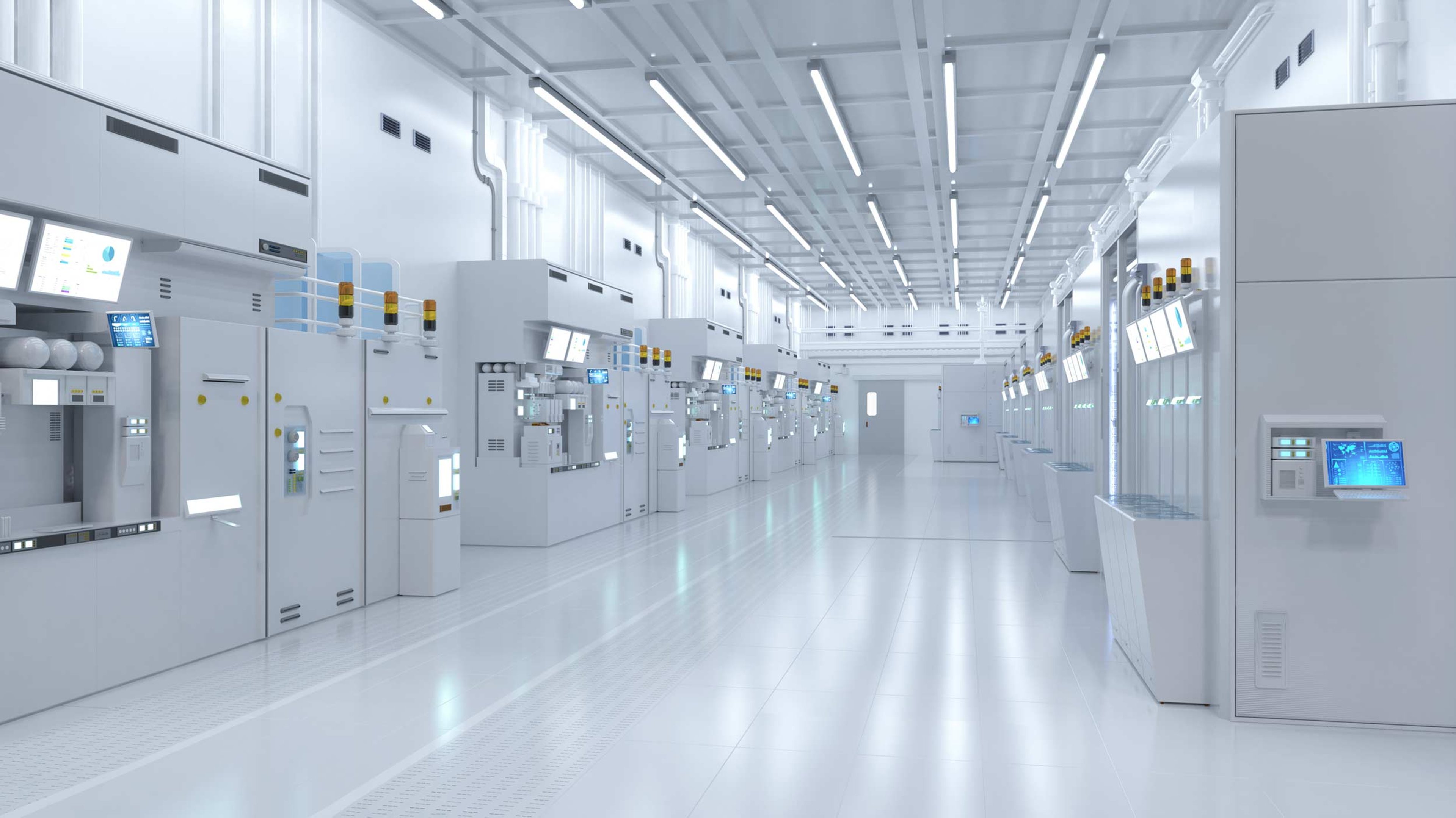
Cleanrooms function as highly controlled production environments where airflow, temperature, humidity, and particle levels are continuously managed.
The cleanroom as a precision system
A semiconductor cleanroom is often described as a room. In practice, it functions more like a gigantic factory sized machine.
Air is supplied through ceilings engineered for uniform flow and particle control. Pressure gradients are tuned to protect the most sensitive process areas. Heat from tools is balanced against airflow and humidity requirements that can include dew points as low as minus 50 degrees Celsius. Air temperature stability reaches plus or minus 0.001 Kelvin, with humidity controlled to tenths of a percent.
Exyte brings more than fifty years of experience in cleanrooms and controlled environments to this task. These spaces are designed not as architectural shells, but as production systems that must perform continuously, across multiple technology generations.
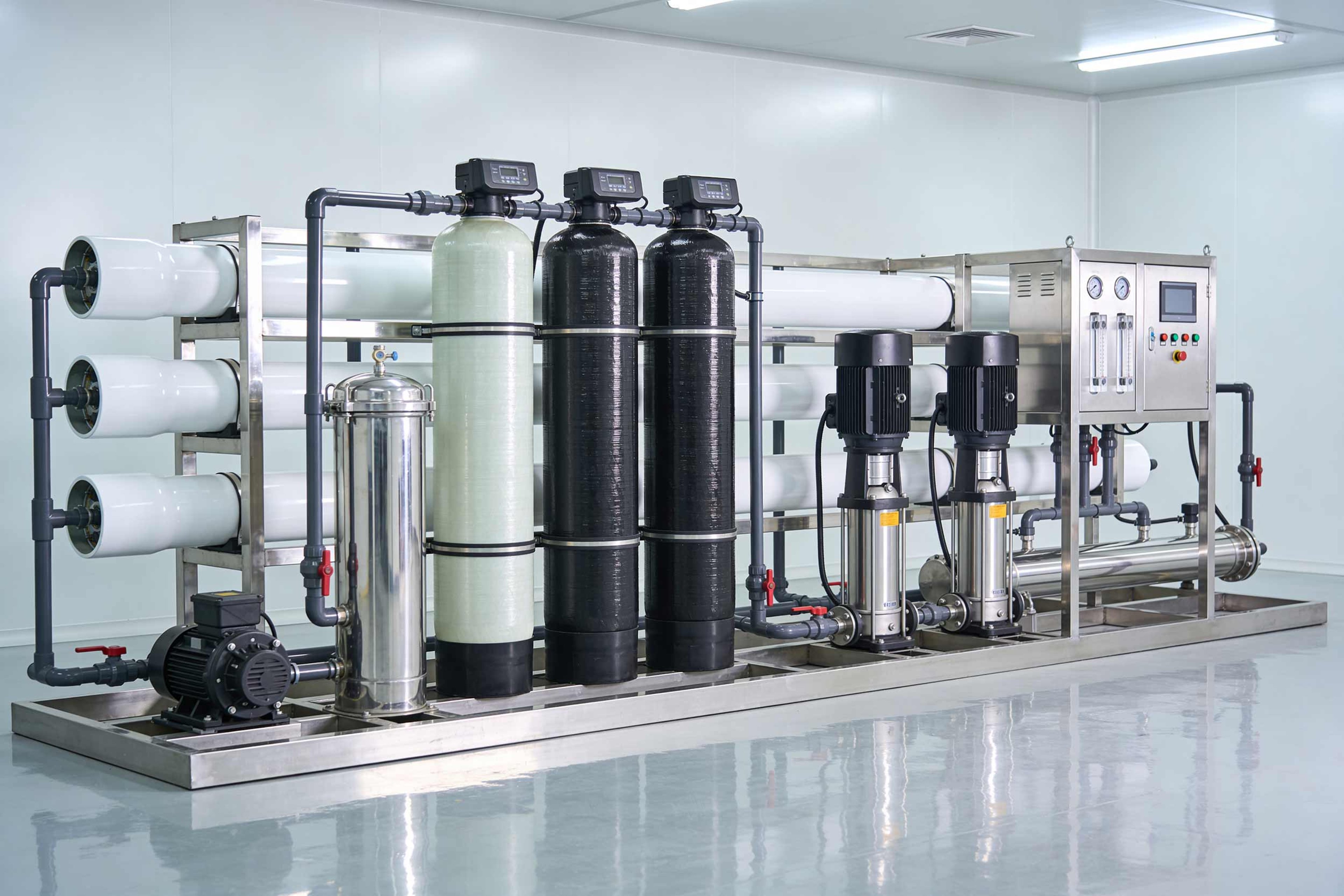
Semiconductor manufacturing relies on extensive utility systems, including ultra-pure water, specialty gases, process chemicals, and waste treatment infrastructure.
The systems behind the process
Beyond the tools themselves, semiconductor manufacturing depends on what are known as critical subsystems. These are the systems that deliver what the process needs and safely remove what it produces.
They include the supply of high-purity chemicals and specialty gases, the exhaust and treatment of by products, and the infrastructure that prevents cross-contamination or unplanned exposure. If these systems fail or drift, production stops or yield is lost.
In a typical fab, this translates into tens of thousands of physical and functional connections. With up to 2,000 tools on site and dozens of interfaces per tool, the facility must coordinate well over 100,000 individual supply and disposal points for power, gases, chemicals, water, exhaust, and data.
Exyte engineers these subsystems as part of the overall factory, not as isolated add‑ons. Through its integrated subsidiary Exentec, the company also delivers key technologies that go directly into the fab, including cleanroom products, air handling units, exhaust systems, gas abatement, skids, and on‑site installation services for mechanical, electrical, and process systems.
Much of this infrastructure is invisible during operation. Its success is measured by how reliably it works.
Utilities that never draw attention
If a fab’s utilities become noticeable, something has already gone wrong.
Electrical systems must deliver stable power under highly variable tool loads. Cooling and process water must meet strict chemical and thermal limits. Supply and exhaust systems must operate continuously without disrupting production.
Exyte designs these systems with redundancy and operational continuity in mind. Mechanical and electrical distribution is arranged so that servicing can take place while the fab remains live. Performance is verified through structured commissioning, qualification, and validation.
Engineering for speed and consistency
A modern fab is often built for equipment that is still evolving during the design phase.
To manage this, Exyte relies on global concept development and close collaboration across regions. Teams in Asia, Europe, and North America work from shared engineering principles, allowing fast‑track project execution while maintaining consistent quality across locations.
Dynamic virtual simulation is part of this early engineering work. Energy use, emissions, and resource consumption are modeled during design to predict real operating behavior. During commissioning and qualification, these predictions are validated against actual performance to confirm that the factory behaves as planned.

Exyte delivers semiconductor facilities through an integrated approach spanning engineering, construction management, installation, commissioning, and qualification.
Integration across the full factory scope
Constructing a semiconductor fab is not only an assembly exercise. It is one of the most complex industrial undertakings today. It is an integration challenge. Each connection is part of a tightly interdependent network, meaning the factory itself operates as a single, highly complex system.
In this sense, the fab is not just a building housing production tools, but a sophisticated machine in its own right. One that must function as a whole from day one.
Exyte’s scope covers consulting and planning, engineering and design, project and construction management, procurement, installation, and commissioning. This includes cleanrooms, facility plant equipment, process system distribution, electrical infrastructure, manufacturing automation interfaces, and tool installation.
With a track record of more than four million square meters of semiconductor production space commissioned worldwide, and decades-long contributions to the development of modern microelectronics infrastructure, this integrated approach has proven to reduce risk at the point where delays are most costly.
From first power to first wafer
As a fab approaches completion, construction gives way to proof.
Systems are tested under load. Environmental conditions are measured and documented. Control strategies are verified. Only then does the factory transition to tool hookup and production ramp up.
The first successful wafer run is not a milestone that appears by chance. It is the visible result of infrastructure that already works.
The infrastructure behind progress
Advances in semiconductor technology are often attributed to breakthroughs in physics or equipment design. Those advances depend on factories that can deliver extreme precision, every day, and at scale.
Exyte works in this space. Serving some of the most technically demanding clients in the industry, the company operates in more than twenty countries to turn empty sites into functioning semiconductor fabs.
When a wafer moves smoothly through a production line, it is passing through an environment that has already done its work.
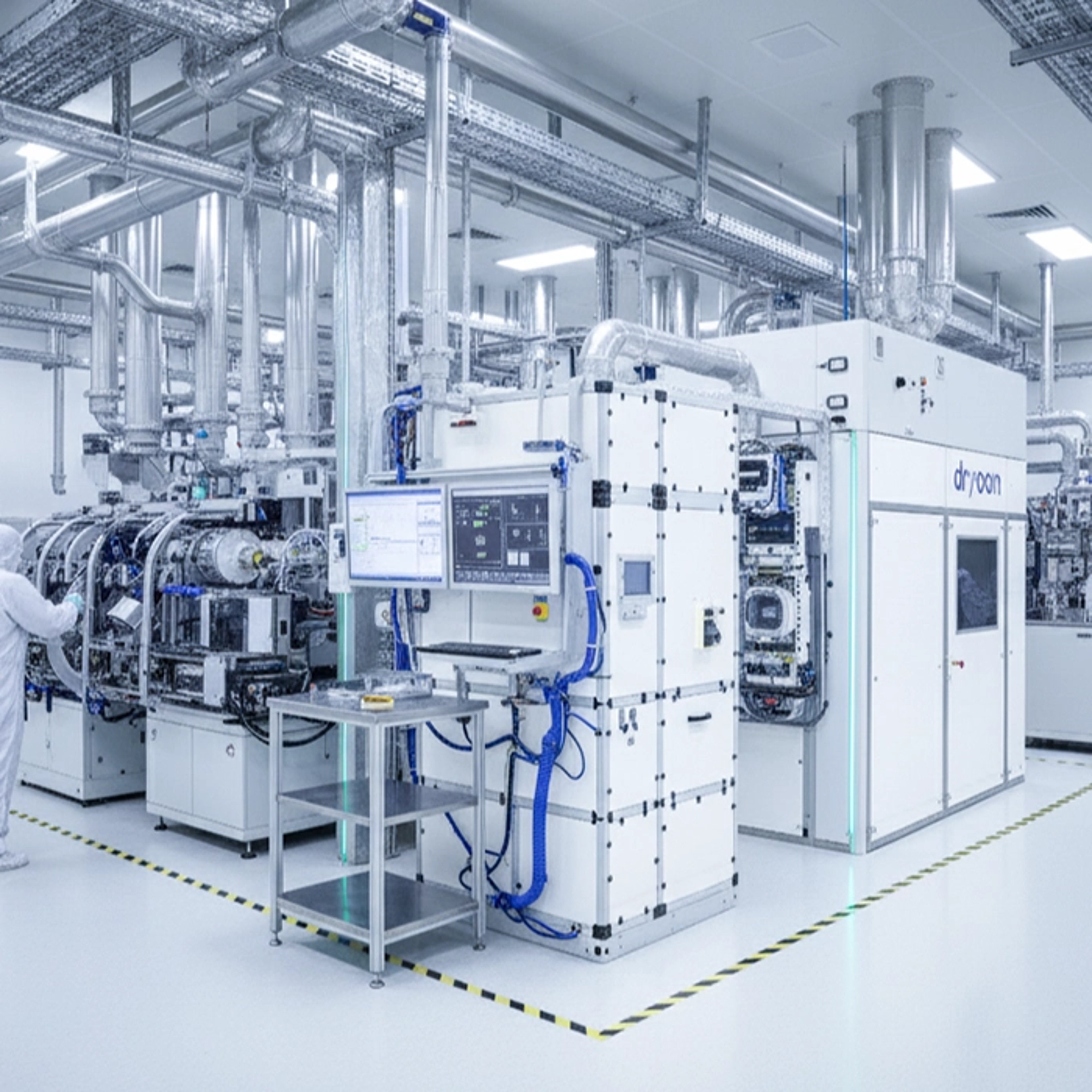
Off-site Manufacturing
Exyte's Off-site Manufacturing (OSM) approach enables more predictable delivery of complex facilities through modularization, standardization and industrialized execution. Discover how OSM supports accelerated project delivery across semiconductors, biopharma and life sciences, batteries and data centers.